ASIC VGA Controller
By Mark Bowers and Michael Prechel
April 24, 2013
For our final project in Dr. Abdel-Aty-Zodhy's ECE585 VLSIC Design of Digital Chips at Oakland University, Michael Prechel and I designed a VGA graphics controller written in Verilog and implemented as an application-specific integrated circuit.
Layout of the VGA ASIC
I had previously implemented VGA on 68HCS12 and PSoC 1 microcontrollers using minimal external components, by essentially emulating the VGA standard in software. This was an interesting proof-of-concept, but it takes a considerable amount of CPU resources (nearly 95% continuous utilization!) to meet the strict timing and bandwidth requirements of the VGA standard. Needless to say, if you want to properly drive a VGA monitor, it behooves you to use hardware specifically designed for this task. This was the motivation behind our design.
Our VGA ASIC continuously displays the contents of an SRAM display buffer to a monitor adhering to the VGA 640x480 standard. It is also provides a SPI interface through which the contents of the SRAM buffer can be modified by a microcontroller. Thus, the microcontroller is no longer responsible for producing the timing-sensitive VGA signal. Nor is it bogged down by merely displaying a static image; it is only busy when modifying the video buffer over the SPI interface.
VGA is essentially a massive multiplexed display. For a 640x480 display, the pixel is changed at a rate of 25.175MHz. Each line consists of 480 pixels, but also contains some “blanking” time (historically this was time needed for the CRT deflection coil to sweep back to the beginning for the next line.) There is also a blanking time necessary to return the coil to the top of the frame after reaching the bottom.

VGA standard diagram (Source: Xilinx)
VGA timing tables (Source: tinyvga.com)
| Scanline part | Pixels | Time [µs] |
|---|---|---|
| Visible area | 640 | 25.422045680238 |
| Front porch | 16 | 0.63555114200596 |
| Sync pulse | 96 | 3.8133068520357 |
| Back porch | 48 | 1.9066534260179 |
| Whole line | 800 | 31.777557100298 |
| Frame part | Lines | Time [ms] |
|---|---|---|
| Visible area | 480 | 15.253227408143 |
| Front porch | 10 | 0.31777557100298 |
| Sync pulse | 2 | 0.063555114200596 |
| Back porch | 33 | 1.0486593843098 |
| Whole frame | 525 | 16.683217477656 |
| Portion | Rate |
|---|---|
| Vertical Refresh | 60 Hz |
| Horizontal Refresh | 31.46875 kHz |
| Pixel Clock | 25.175 MHz |
The following block diagram illustrates the architecture of the VGA controller:
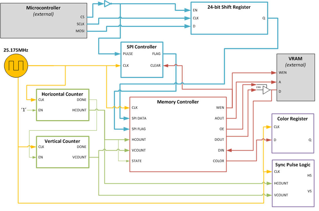
VGA controller block diagram
The VGA controller continuously displays the contents of the VRAM. This is achieved with the use of a horizontal counter (controlling the timing of each line), and a vertical counter (controlling the timing of the frame.) The counter values are combined to yield the VRAM read address. The counter values also pass through comparators to produce “sync pulses” which are part of the VGA standard (used by the monitor to lock-on to the VGA signal.)
Meanwhile, the microcontroller can shift-in a 24-bit command via SPI, consisting of an X coordinate, Y coordinate and the color to be written to the display buffer. Upon completion of the SPI cycle, the memory controller interleaves in the pending VRAM write. It performs the VRAM write quickly between successive VRAM reads. VRAM reads pass through a register, so that writes (which happen asynchronously, relative to the display routine) will not cause any blips or artifacts on the monitor.

SPI controller state machine
The SPI state machine stays in the "idle" state until an incoming SPI word has been shifted in. The SPI cycle begins when CS (chip select) is brought low. The master (microcontroller) then shifts in data using MOSI and SCLK. When CS is brought high, the cycle ends. At this time, the SPI controller then sends a VRAM write command, and waits for this write to be serviced. The write command is 24-bits, consisting of three bytes: color, X coordinate and Y coordinate. Once the write is completed, the system is again idle and can service another write. The “wait for write to be serviced” state is necessary so that the VRAM may be written to safely, without interfering with the display routine. The VRAM is being continuously juggled between (1) reading out to the monitor, and (2) possibly servicing a pending write.
The memory “juggling” behavior is achieved in the memory controller state machine. The current state is derived from the two least significant bits of HCOUNT.
In state 0, the DOUT driver is disabled (i.e. the RAM data bus is being read from), and the read address output is output. In state 1, the memory controller waits a cycle for the VRAM to fetch the data at that address. In state 2, the memory controller registers the VRAM read, and the color becomes visible on the VGA port (by registering the VRAM read, this ensures that the monitor will not see the write transaction.) Also in this state, if an SPI write is pending, the DOUT driver is enabled (i.e. the RAM data bus is being written to), the write address is output, and WEN is asserted. In state 3, WEN is deasserted. This state is necessary to meet the write hold timing, and to ensure that we do not inadvertently write at a read address.

Memory Controller State Diagram
Several logic simulations were performed to verify that the VGA timing and SPI interface worked as intended:

Simulation of the SPI write-to-VRAM operation. A SPI command has finished (rising edge of CSn). This is detected and raises the SPI flag register. The memory controller interleaves this write between reads. After the write is serviced, the SPI flag returns low.
Simulation of VGA Frame Timing
Simulation of VGA Line Timing

Simulation of three horizontal lines. When the horizontal counter reaches the maximum value, the comparator "Hdone" output goes high; this resets the horizontal counter and increments the vertical counter.

Simulation of the sync pulse width
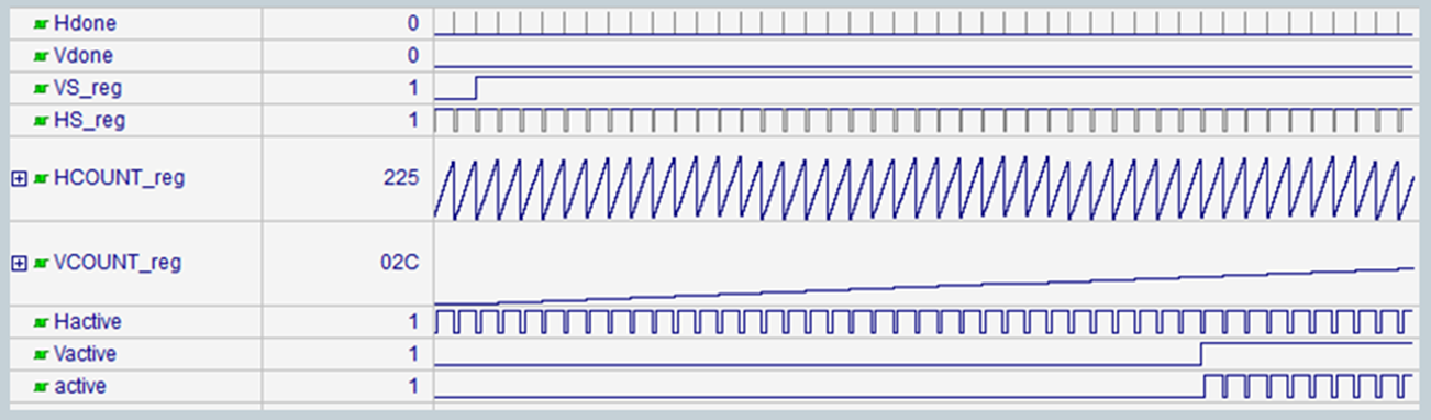
Simulation of several lines of video, illustrating the behavior of the "active" signal, which indicates whether or not a line of video contains visible information, or is part of the blanking period (the time when the electron beam is sweeping back. If it is part of the blanking period, then the color output is grounded, as per the specification.
The Verilog design was then compiled for a Mercury FPGA development board, which contains a Xilinx Spartan-3A 200K FPGA, to emulate the behavior of the VGA ASIC. (The design only consumed 3% of the FPGA logic resources!) The Mercury board also contains a Cypress 512K x 8bit SRAM, which was used as the video buffer. It was connected to a Dragon12 HCS12 development board, which acted as the SPI master. An external 25.175MHz oscillator was used for the clock input.
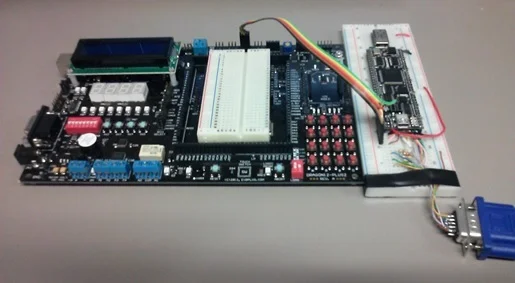
VGA ASIC prototype using a Mercury FPGA module
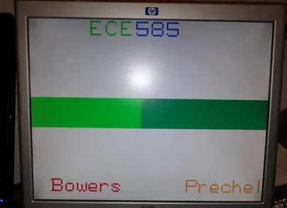
Successful output from the FPGA-based prototype
The Verilog design was then compiled into standard cells using Leonardo:

Leonardo Compilation Report
The timing properties of the design were then analyzed. The critical path is 6.49 nanoseconds, yielding a maximum operating frequency of 154 MHz.

Leonardo Timing Report
Below are some images of the logic schematic as generated from the Verilog code:


The standard cells were then placed using the auto-place feature:

Standard Cells Placed
Next, the standard cells were auto-routed:

Standard Cells Routed
Next, some checks were performed on the auto-routed design. No shorts were found! However, four nets "overflowed" by straying outside the specified area. This is tolerable because the specified area was conservative and there is still ample space for routing to the pads.

No shorts found in the auto-routed design!

Four overflows found in the auto-routed design.
Next, Design Rule Checking (DRC) was performed. After running DRC, the auto-routed design showed 36 errors. Most of these errors were metal spacing errors, or vias placed too close together. Correcting these errors was a bit time consuming, but straightforward using skills we learned earlier in lab tutorials.
After correcting all the DRC errors, the design was measured to be approximately 2205 λ x 2625 λ. This fits easily in the 3000 λ x 3000 λ limit for our process.

Auto-routed design. DRC errors corrected manually.